SMD component history
SMD components were developed in the 1960s as a way to reduce the size and weight of electronic devices and to improve their reliability. They became widely used in the electronics industry in the 1980s and 1990s, as surface mount technology (SMT) became more prevalent. Today, SMD components are found in a wide variety of electronic devices, including smartphones, laptops, and other consumer electronics, as well as in industrial, military, and aerospace applications.


Surface mount technology
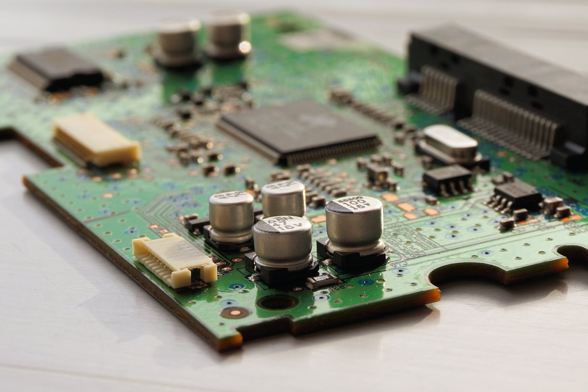
Surface mount technology (SMT) is a method of constructing electronic circuits in which the components are mounted or placed directly onto the surface of printed circuit boards (PCBs). It was developed in the 1960s as a way to reduce the size and weight of electronic devices and to improve their reliability.
SMT became widely used in the electronics industry in the 1980s and 1990s, as manufacturers sought to increase the density and complexity of circuits while reducing the cost and time required to assemble them. The use of SMT allowed for the production of smaller and more lightweight electronic devices, and also made it possible to automate the assembly process, leading to further cost savings.
Today, SMT is the dominant method of assembling electronic circuits, and is used in the production of a wide variety of electronic devices, including smartphones, laptops, and other consumer electronics, as well as in industrial, military, and aerospace applications.
Standards used for SMD:
There are several standards that apply to surface mount devices (SMDs) and surface mount technology (SMT). These standards provide guidelines for the design, production, and testing of SMDs and SMT assemblies. Some examples of SMD standards include:
- IPC-J-STD-001: This is a standard developed by the Institute for Interconnecting and Packaging Electronic Circuits (IPC) that provides guidelines for the soldering of electronic components to printed circuit boards (PCBs). It covers a wide range of topics, including materials, process control, inspection, and testing.
- IPC-A-610: This is another standard developed by the IPC that provides acceptance criteria for the inspection of electronic assemblies. It covers topics such as workmanship, component placement, soldering, and cleaning.
- IPC-7351: This standard provides guidelines for the design and development of land patterns for surface mount devices (SMDs). It includes information on the dimensions and shapes of the pads that the SMDs are soldered onto, as well as guidelines for the spacing between pads and other design considerations.
- JEDEC: The Joint Electron Device Engineering Council (JEDEC) is an organization that develops standards for the design and testing of electronic components, including SMDs. Some examples of JEDEC standards that apply to SMDs include JEDEC MO-220, which covers the mechanical dimensions of surface mount packages, and JEDEC MO-220-WL, which covers the dimensions of wafer-level packages.
SMD components size
Surface mount devices (SMDs) come in a range of sizes, with dimensions that are typically measured in millimeters. The size of an SMD component is typically specified by its width and length, as well as its height or thickness.
Some common sizes for SMD components include:
- 0201: This is a very small SMD component, with dimensions of 0.2 mm x 0.1 mm. It is used in applications where space is extremely limited.
- 0402: This is a slightly larger SMD component, with dimensions of 0.4 mm x 0.2 mm. It is still relatively small and is often used in compact electronic devices.
- 0603: This is a medium-sized SMD component, with dimensions of 0.6 mm x 0.3 mm. It is widely used in a variety of electronic applications.
- 0805: This is a larger SMD component, with dimensions of 0.8 mm x 0.5 mm. It is often used in applications where a bit more space is available.
- 1206: This is a larger SMD component, with dimensions of 1.2 mm x 0.6 mm. It is often used in applications where a moderate amount of space is available.
- 1210: This is a larger SMD component, with dimensions of 1.2 mm x 1.0 mm. It is often used in applications where a moderate amount of space is available.

SMD components package
There are many different types of SMD component packages, each with its own unique shape and size. Some common types of SMD packages include:
- Dual in-line package (DIP): A rectangular package with two rows of pins.
- Small outline package (SOP): A rectangular package with a single row of pins.
- Quad flat package (QFP): A square or rectangular package with pins on all four sides.
- Ball grid array (BGA): A package with a grid of balls on the bottom that make contact with the PCB.
- Plastic leaded chip carrier (PLCC): A square package with leads that extend from the sides.
The package of an SMD component will typically be indicated by a series of letters and numbers that are printed on the component itself, or on the packaging it came in. For example, a QFP package might be labeled as “QFP-64,” indicating that it has 64 pins.
It’s important to choose the appropriate package for your application, as the package will determine the size and shape of the component, as well as the number and spacing of the pins. Choosing a package that is too large or has too many pins may make it difficult to fit on your PCB, while a package that is too small or has too few pins may not provide the necessary connectivity or functionality.
